 Well-known PCB supplier
+8618879561688
1. We can do 68 layers PCB assembly, mimi track/spacing: 2.5/2.5mil, max board thickness hole size:16:1.
2. Long and short Golden finger assembly tech and high density circuit accuracy control, meet the light and communication area's PCB design requirement.
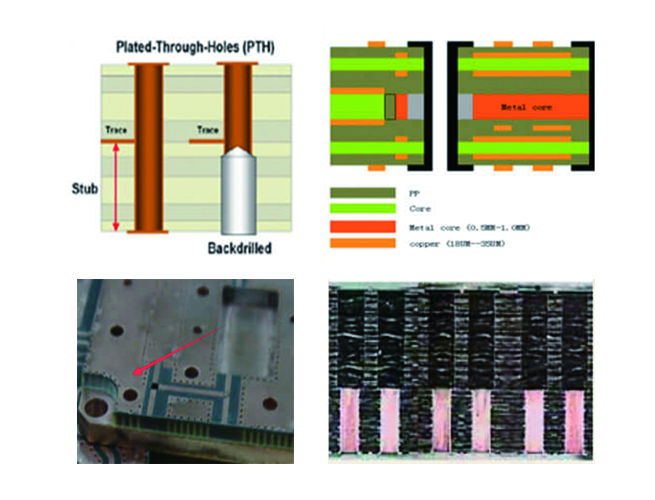
3. High precision back drilling technology reduces the equivalent series inductance through the hole to meet the integrity requirements of product signal transmission.
4. Excellent metal base and ultra-thick copper manufacturing process to meet the high heat dissipation requirements of power products.
5. High precision mechanical and laser depth control technology, to achieve multi-step slot product structure, to meet the assembly requirements of different levels of products.
6. The mature mixed pressing process realizes the mixing of FR-4 and high-frequency materials, which saves material cost for customers under the premise of meeting the high frequency performance of products.
7. Advanced Anti-CAF technology, greatly improves the reliability and life of PCB products.
8. Leading buried capacitance, buried resistance technology, greatly improve the performance of PCB products.
9. Professional R&D of PCB prototype factory, fully automated high-volume factory, to achieve prototype and high-volume orders highly customized, improve efficiency, reduce costs.


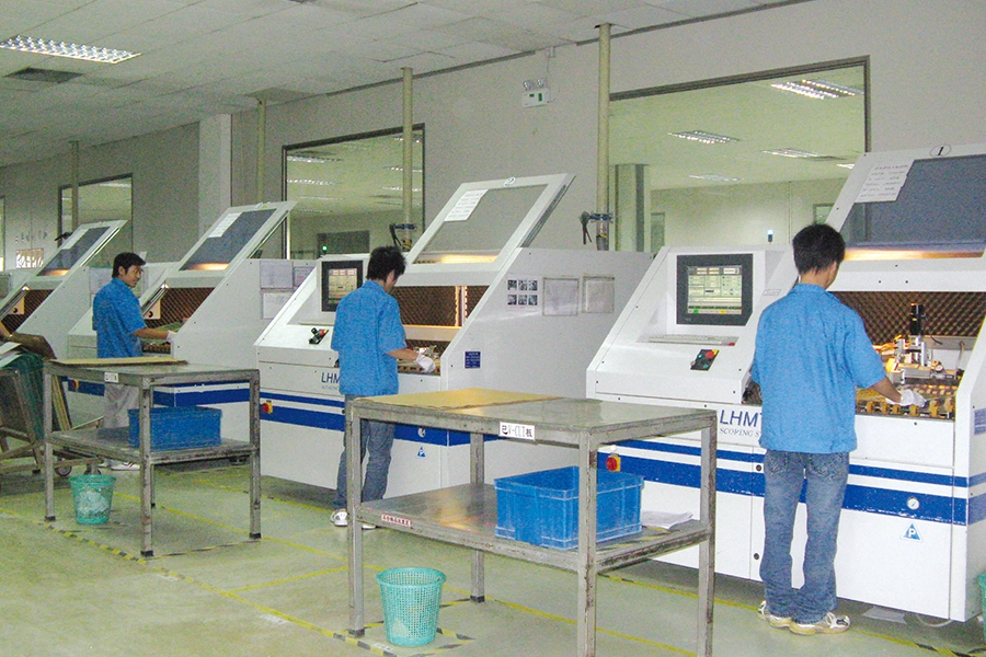
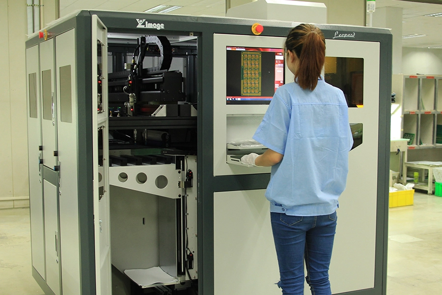
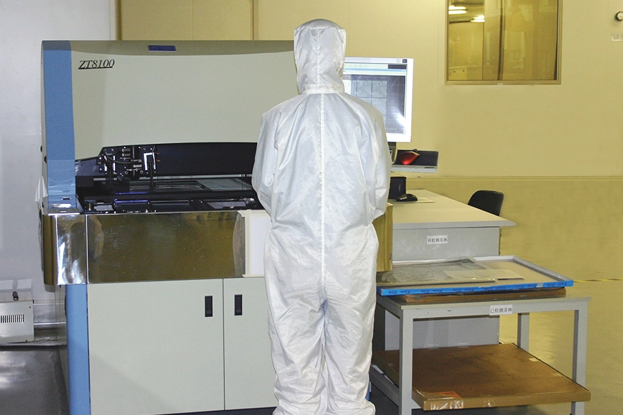
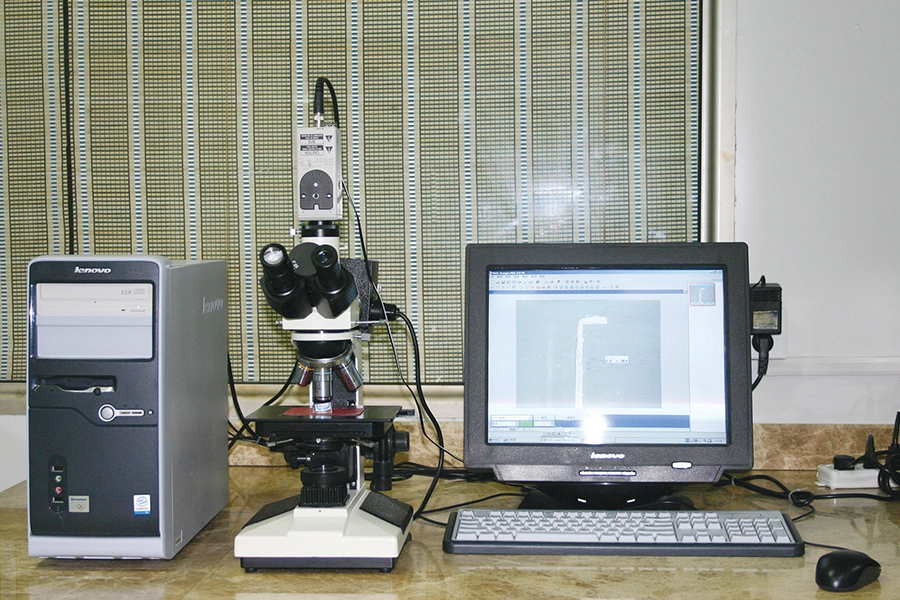
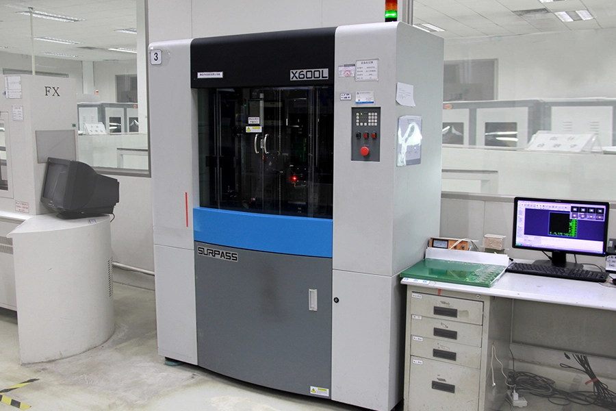
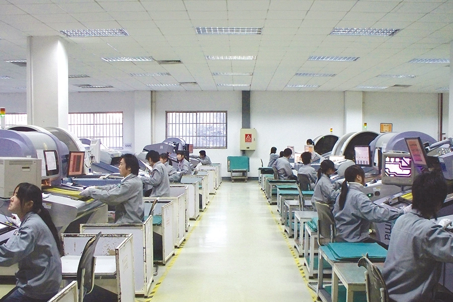
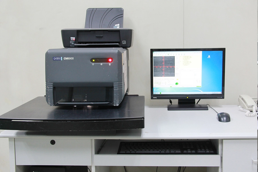
1. AOl(Automatic Optical Inspection) imported from Israel for the inspection of high precision PCB circuit.
2. High precision impedance tester imported from the USA for PCB impedance test.
3. Advanced PLASMA plasma treatment for hole wall cleaning of high-frequency materials such as PTFE and ceramic fillers.
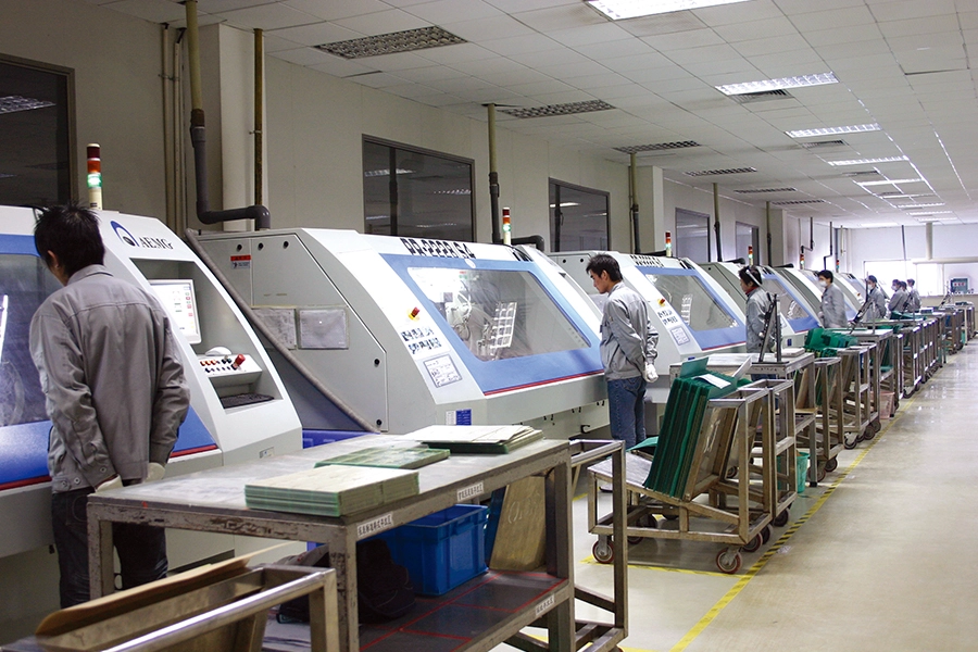
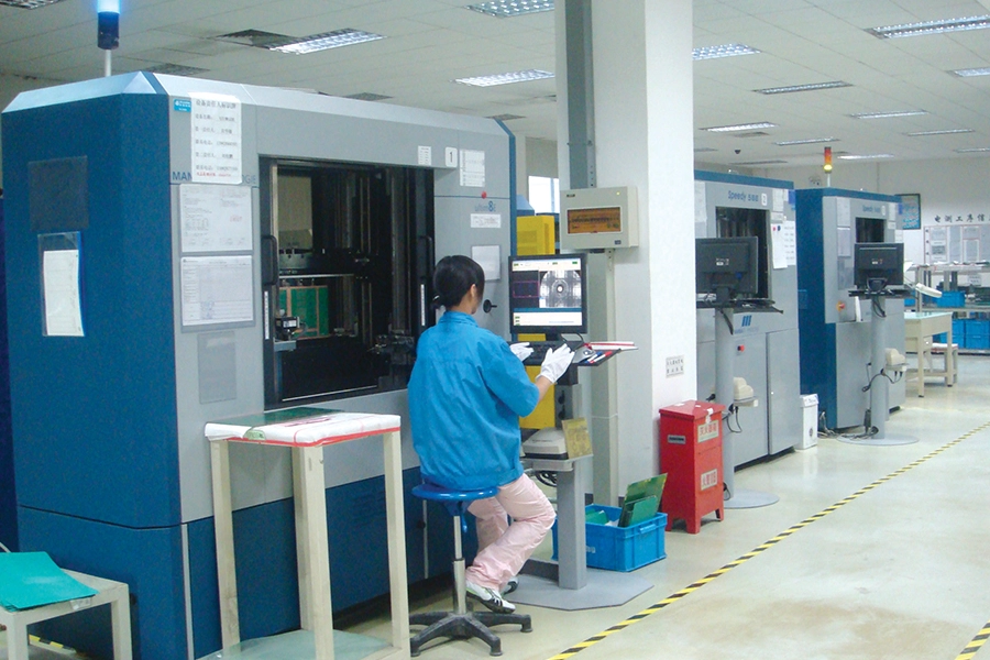
4. Taiwan imported CNC drilling machine, used for back drilling, deep hole control, slot processing.
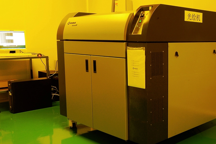
5. Israel imported LDI exposure machine (laser imaging) for the graphics transfer process of high-precision circuit.
6. The CNC forming machine imported from Taiwan is used for deep control milling of PCB with step slot structure.
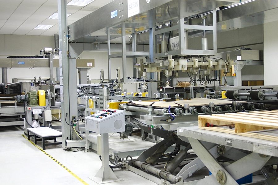
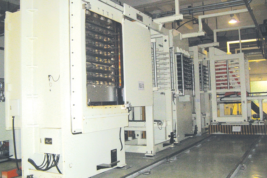
7. BURKLE press imported from Germany for pressing high layer PCB boards.
8. Vacuum resin hole jack, used for high precision circuit BGA hole plugging process.
9. A variety of reliability testing equipment such as ion stain degree tester, anti-stripping strength tester, pore copper tester, secondary element tester, gold thickness tester, etc., strongly ensure the quality of customers' PCB products.
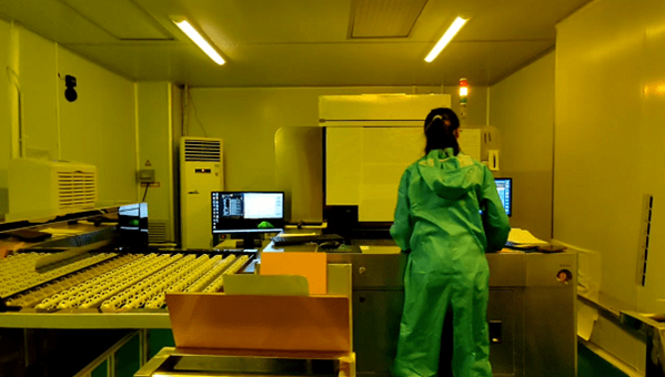
Our intention is to ensure that our products will be performing according to customer’s expectations and that they will be of high quality standard.
We instantly import advanced equipments and advanced technology,dedicated in producing 2-68layer PCB,widely used in computer,avigation,industry.....
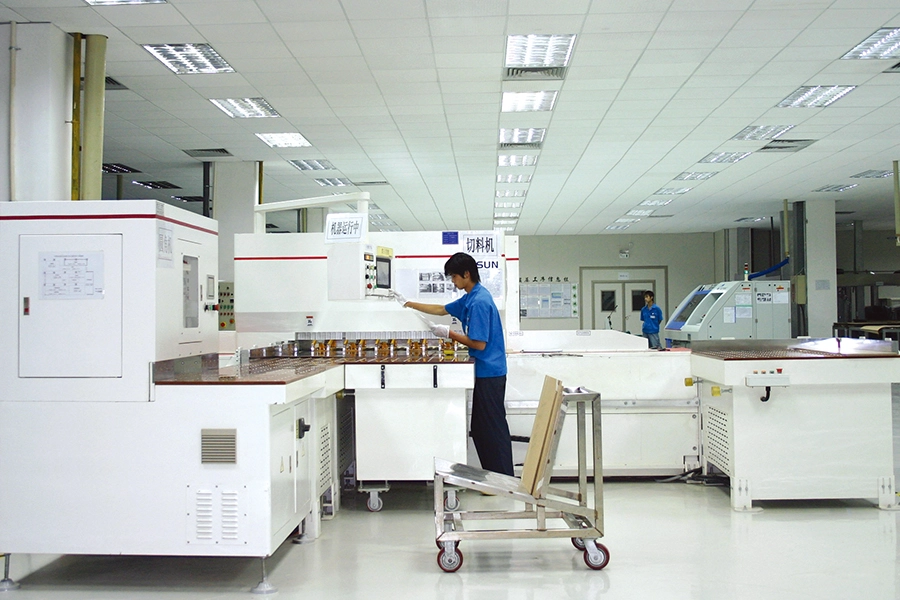
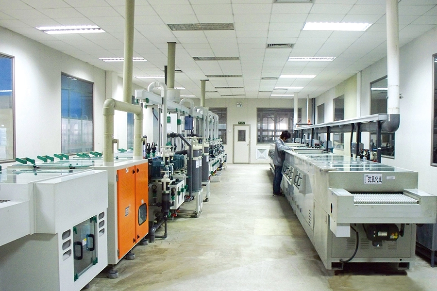
Connect to a OMNI PCB engineer to support your project!
Request A Quote