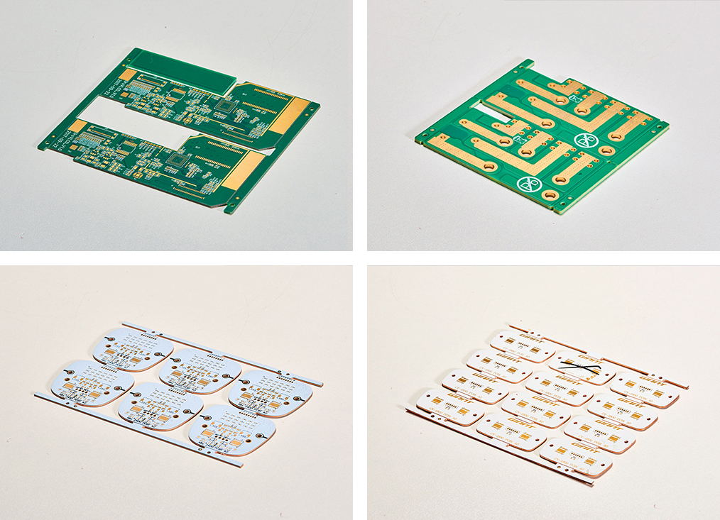
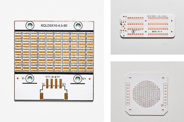
What Is Copper Based PCB?
Copper-based PCB or copper core PCB is a metal core PCB that uses copper as the base material in place of
commonly used FR4. Like all metal core PCBs, it also has three main layers. The top layer is made of copper,
which is responsible for the electrical connection between the components. This layer is standard in all types
of PCBs. The second layer is the dielectric layer that prevents current from the top layer to the base layer.
Although this layer is electrically an insulator, it is a good conductor of heat. It transfers the heat produced
by the components and helps in heat dissipation. The bottom layer of the PCB is copper, which is why it is a
copper core PCB.
Advantages of Copper Based PCB:
1). The thermal conductivity of copper PCB is twice that of aluminum PCB. The higher the thermal conductivity,
the higher the heat conduction efficiency and the better the heat dissipation performance.
2). Due to the difference in the elastic modulus of copper and aluminum (the elastic modulus of copper is about
121,000 mpa, and the elastic modulus of aluminum is 72,000 mpa), the corresponding buckling degree and expansion
and shrinkage of copper based PCB board will be smaller than that of aluminum substrate, and the overall
performance is more stable.
3).copper PCB can be processed into metallized holes, but aluminum can not, the network of metallized holes must
be the same network, so that the signal has a good grounding performance, and copper itself has weldability, so
that the design of the structural parts can be selected for the final installation of welding.
4).Copper-based PCB of copper-based PCB board can etch fine graphics and process them into a boss shape.
Components can be directly attached to the boss to achieve excellent grounding and heat dissipation effect;
Copper based PCB board design rules: due to the copper based PCB is thicker, the minimum diameter of the
drilling tool must be 0.4mm, the line width spacing according to the copper foil thickness on the copper based
PCB board to determine, the thicker the copper foil thickness, the need for the most thin line width is wider,
the need for the minimum spacing must be greater.
Copper Base PCB Design Guide
The minimum drilling diameter needs to be 0.4mm because of the thicker copper base; the copper foil’s thickness
on the copper-based PCB determines how the line width and spacing are. If the copper foil is thicker, it will
need a more expansive line width and larger minimum spacing.
Cost-saving is a prerequisite for copper-based PCB design, especially when designing irregular copper-based
PCBs. Intricate circuit design mainly pay attention to the following factors: routing, aesthetics, assembly,
heat, force, signal, and other requirements;
Force: The external force and vibration that the copper-based PCB receives during the working process, the size
and position of the holes on the PCB Board need to be arranged reasonably, and the weakest surface of the board
caused by the irregular holes should be sufficiently resistant to bending strength;
Routing, aesthetics, assembly: it needs to meet the customer’s visual sense.
 Well-known PCB supplier

